Compute
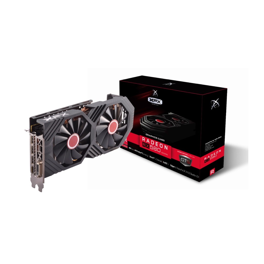
XFX RX 580
Project 06 · Hardware / runtime · October 2026
An externally powered RX 580, an M.2-to-PCIe riser, and a Realtek USB storage bridge became a working GPU training system.
A custom userspace runtime initialized the card and ran the model's FP32 forward pass, backward pass, and AdamW updates on the GPU. The host prepared inputs, managed the run, and wrote checkpoints.
Explore the source ↗01 / The completed run
203,920 optimizer updates. Final held-out cross-entropy: 3.9263 nats/token.
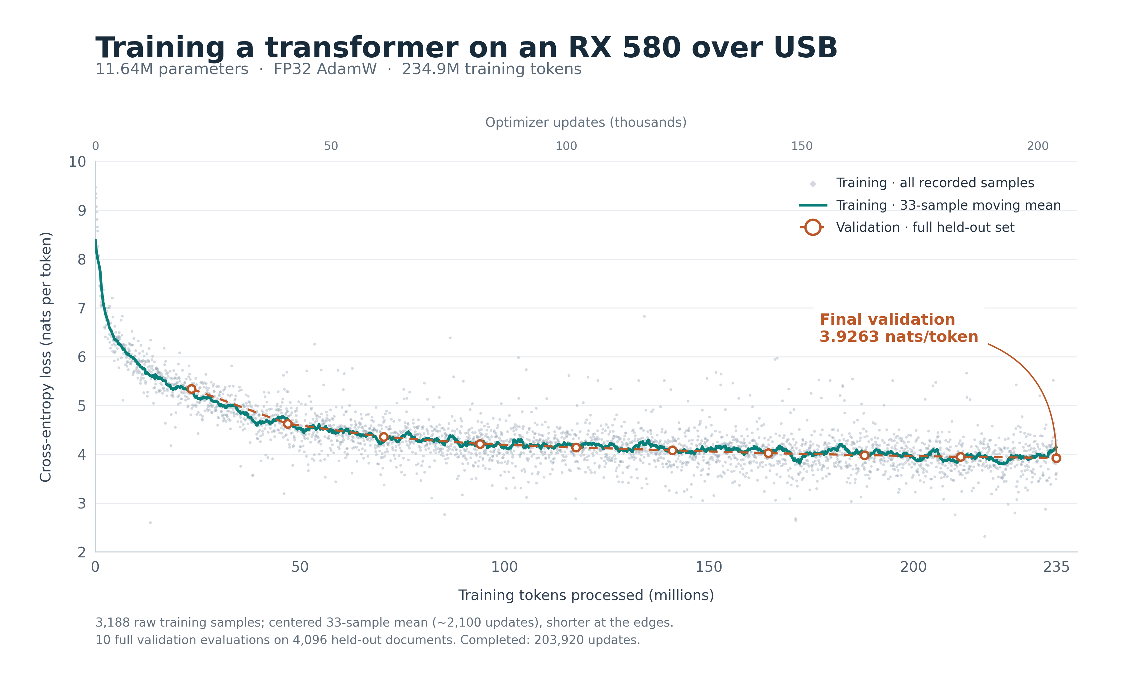
The model had 11,637,760 unique parameters: six layers of width 320, ten attention heads, tied embeddings, a 12,096-token byte-level BPE vocabulary, and a 1,152-token context. Microbatch size was one.
A late-run reporting interval reached 6,533.633 tokens/s. That is a measured interval, not the whole-run average. The run crossed implementation revisions and development interruptions. Final validation was 1.42976 bits per raw UTF-8 byte.
02 / Hardware
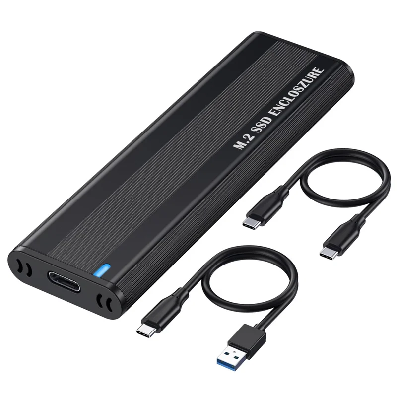
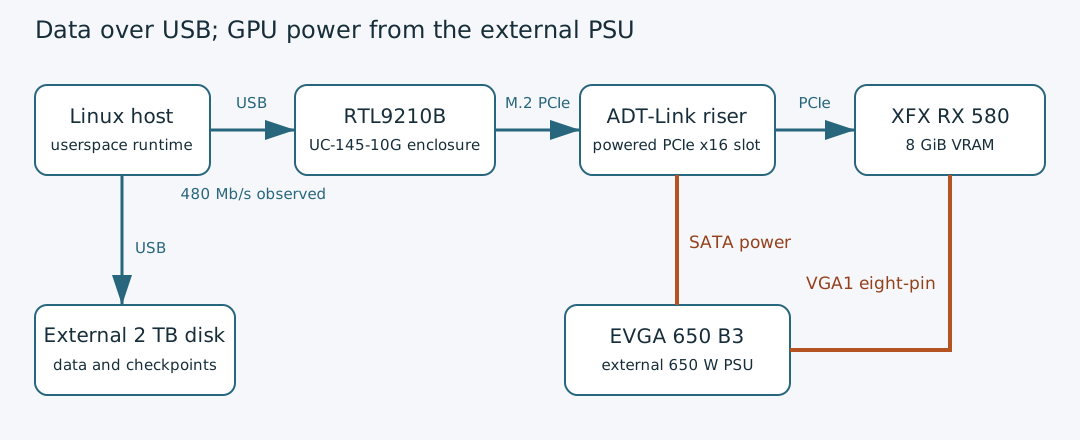
The enclosure's M.2 socket held the riser connector, not an SSD. A separate external drive stored data and checkpoints.
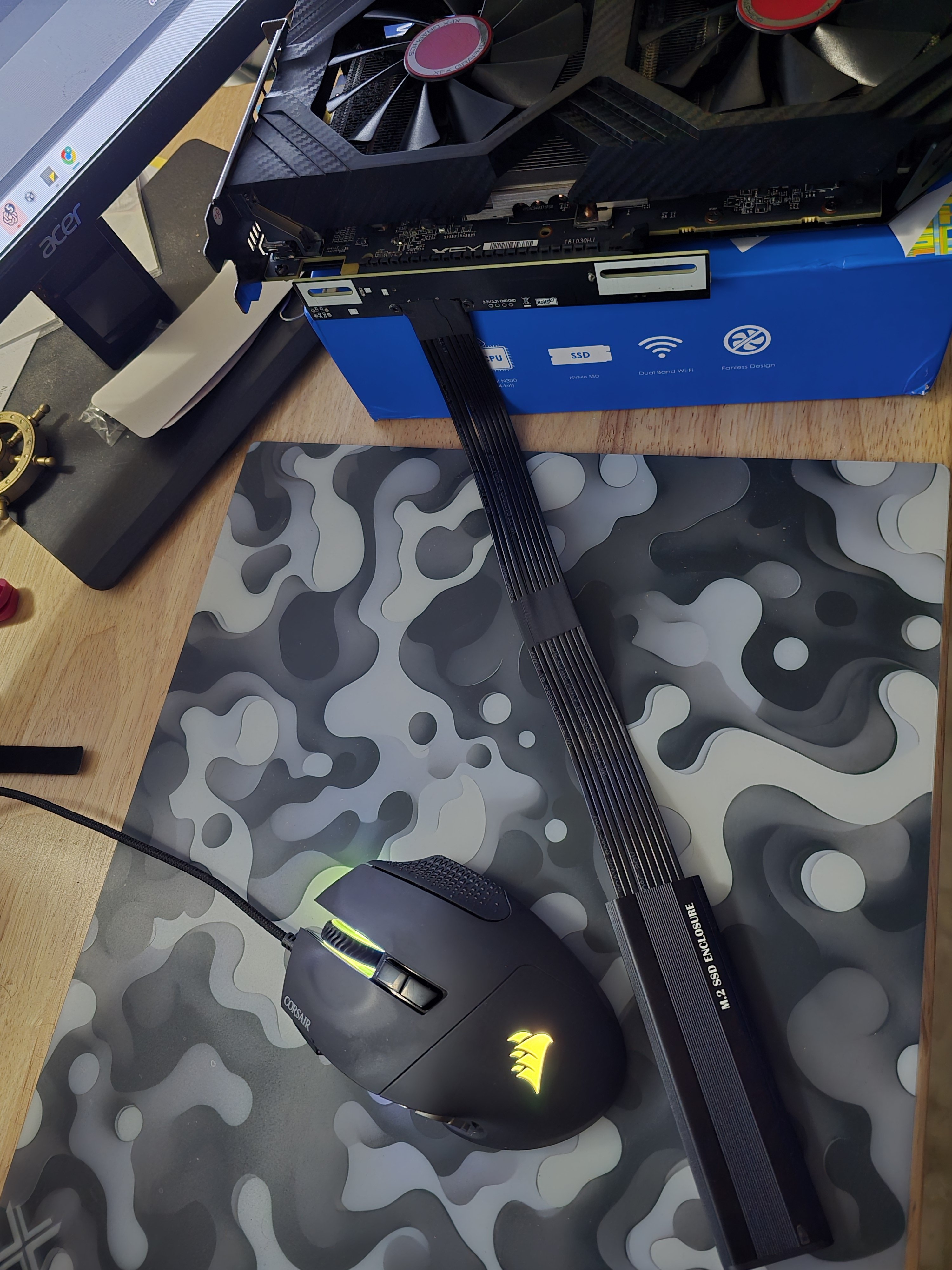
The actual assembly
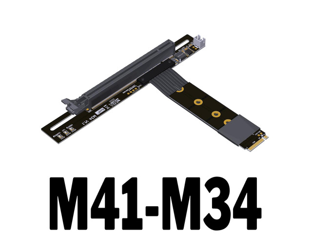
The riser's M.2 connector fits where the SSD normally sits, but its cable still needs a way out. The enclosure tray's rear plate was cut off with scissors so the cable could slide in.
This was a physical modification to the enclosure tray—not to the GPU backplate, bridge firmware, or GPU VBIOS. The ribbon cable connects the enclosure to the riser beneath the card; the separate PSU supplies the GPU and powered slot.
The photograph shows the real hardware arrangement. The product images below identify the individual components.
Compute
USB bridge
PCIe connection
External power
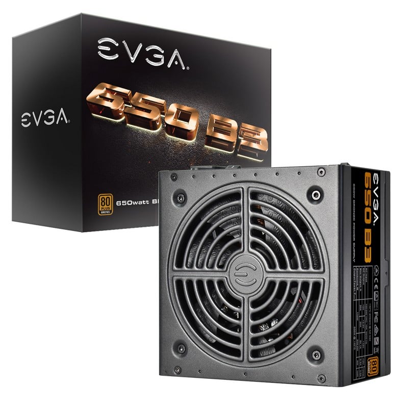
Product photographs illustrate the components; they are not photographs of the assembled rig. They remain third-party material and are not covered by this project's CC0 dedication.
03 / Making it work
Power LEDs were only the beginning. With no motherboard firmware or normal graphics driver bringing the card up, the project first needed a way to identify it, access its registers, initialize memory, and control cooling.
An offline Java/Ghidra firmware lab explored the enclosure's MIPS code, but stopped at a call into an absent external ROM routine. It was useful for analysis, not a complete enclosure emulator.
Meanwhile, cyrozap's RTL921x reverse-engineering notes documented the stock vendor-command route. Linux SG_IO carried those SCSI commands over USB, exposing the bridge's PCIe transaction machinery. Reading PCI identity led to configuration-space, register, VRAM, and BIOS access—without rewriting flash.
A QEMU/libvfio-user branch presented the physical GPU to a guest. Guest-originated accesses, real writes, interrupts, and a GPU-originated write were demonstrated. But servicing arbitrary GPU-initiated reads from guest RAM was a different problem: the stock storage bridge did not provide a general completion path. Stock amdgpu initialization remained unfinished.
The working training route used a separate design: keep model state, commands, kernel arguments, and execution data in VRAM; explicitly transfer data over USB; and own the device through a small userspace runtime. This is not a working stock amdgpu/ROCm/PyTorch GPU backend. PyTorch supported CPU reference work, initialization, and serialization.
The runtime reused AMD's ATOM BIOS interpreter with the card's BIOS tables and signed Polaris microcode. LLVM compiled OpenCL kernels for gfx803. Explicit queue packets and completion fences made device execution observable.
An early AXPY matched 257 expected outputs and preserved 63 guard values. A small network then exercised forward, backward, update, inference, and checkpoint restore. The transformer backend added embeddings, attention, normalization, matrix operations, gradients, and AdamW over the same buffer, tensor, kernel, and reusable-plan API.
04 / Making it practical
The central performance problem was often how much the host and GPU had to say to each other. Many small USB round trips could leave the card waiting even when the arithmetic itself was inexpensive.
A stock bulk command replaced slow dword uploads. GPU-side SHA-256 then replaced a full payload readback with a small digest, while still checking the complete uploaded bytes and generation.
Resident plans kept command sequences and argument blocks on the card. A sixteen-slot buffered input queue let the GPU consume prepared updates while the host replenished later work. Device-side ownership, checksums, and finite-loss checks removed a host handshake between every useful operation.
Clock traces showed real low-clock intervals, including 300 MHz. Correctly initializing the native current and package-power controllers—and supplying the BIOS TDP in the firmware's expected units—removed those intervals in the paired test. This was stock policy, not an overclock or an increase in voltage or protection limits.
The paired complete update fell from 201.31 to 153.83 ms, with all 304 compared state hashes identical. Sampled kernel clocks after the correction were 1322–1364 MHz. One runtime owner handled USB access, cooling, and telemetry; monitors read its snapshot instead of competing for the transport.
Keeping approximately 13.1 MB of validation token IDs in VRAM let the GPU replay forward plans and return only 11,380 bytes of losses for 2,845 contexts. Warm validation fell from about 19.3 minutes to 2.46 minutes. All loss values matched bit-for-bit, and the compared training state stayed unchanged.
Once per host-clock hour, the harness captures a consistent immutable snapshot at an update boundary. Training resumes while 4-KiB low-priority packets drain through a 1-MiB staging area to a host writer. The single snapshot slot stays occupied through durable publication; a later opportunity is skipped if it is still busy.
This has a short capture boundary, not a zero-time copy of the whole model. The GPU does not schedule its own checkpoints.
05 / Measurements
These are separate retained comparisons, not an end-to-end speedup chain. Their gains should not be multiplied together.
| Workload | Before | After | What changed |
|---|---|---|---|
| 4-KiB upload | 21.414 s | 0.131 s | Dword transactions → stock bulk command. Median of three; exact readback. |
| 1-MiB verified upload | 10.294 s | 5.409 s | Full readback → GPU-side SHA-256 verification. |
| 314 zero-element dispatches | 2.256 s | 0.421 s | Host orchestration overhead, not shader throughput. |
| 128-GEMM cycle | 452.151 ms | 199.712 ms | Synchronous → buffered submission; not a transformer update. |
| Training intervals | 5,133 tok/s | 5,630 tok/s | Generic kernel improvement during the same run: about 9.7%. |
| Paired complete update | 201.314 ms | 153.826 ms | Stock power-controller correction; all 304 compared state hashes equal. |
| Complete validation | 1,157.593 s | 147.769 s | Resident inputs and execution. Warm repeat: 147.339 s. |
| 2-MiB snapshot transfer | 86.329 s | 50.566 s | Immutable-buffer microbenchmark; not a full model checkpoint. |
Validation: residency had a 132.75-second one-time preparation cost. The approximately 7.86× repeat result is a warmed validation improvement, not a training-throughput claim.
Checkpointing: the 2-MiB comparison does not measure a full approximately 139.7-MB model-and-optimizer checkpoint. No unmeasured full-checkpoint speedup is assigned to the asynchronous implementation.
Temperature and power: the late-run interval reported 63°C at 100% fan demand. The thermal cutoff was 80°C. The BIOS package limit was 145 W; package telemetry is not wall-plug power.
Training used 301,898 documents and 931,017,861 raw UTF-8 bytes. One RDQ targeted 80 raw bytes per unique parameter; the frozen prefix landed 2,939 bytes below that target. The held-out set contained 4,096 documents, 3,276,412 tokens, and 12,980,528 raw UTF-8 bytes. Cross-entropy and bits per byte use different denominators.
The source handoff reports successful Docker builds, scheduler lifecycle checks, CPU initialization, and research-tool builds. Those packaging checks are not new GPU experiments. Historical real-device workflows are retained in the source; the original datasets, weights, installed firmware blobs, and raw machine logs are not bundled.
The native runtime build reports 16 existing signedness/pointer-signedness warnings from the pinned upstream ATOM interpreter. The package records that compilation succeeds; this website has not independently rerun the hardware training experiment.
Full results · Recorded measurements · Distribution verification
06 / Source snapshot
The runtime, transformer backend, deployment configuration, and earlier firmware and VM research are available in one browsable release.
Reproduction requires compatible hardware and explicit device configuration. This is a research implementation, not a plug-and-play USB graphics driver. Start with the reproduction guide before any device-access command.